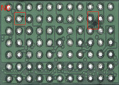
Equipment Applications

Different Applications of Wafer AOI Products
01
Processor Chip
Characteristics:
1.Complex graphical background.
2.Requirement for 3D. measurement of bumps.
3.High defect rejection criteria.

02
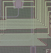
Communication Chip
Characteristics:
1. High detection accuracy in optical port areas.
2. Requirement for measurement of optical port width.
03
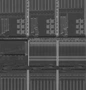
Memory
Characteristics:
1.High number of pads.
2.High pattern repetitiveness.
3. General defect rejection criteria.
04
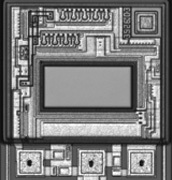
Sensor Chip
Characteristics:
1.High detection accuracy on light-receiving surfaces.
2.Small die size.
3.General defect rejection criteria.
05
Power Management
Characteristics:
1.Noisy background.
2.Many needle marks.
3.General defect rejection criteria.
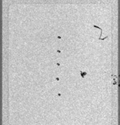
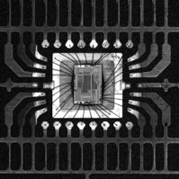
Applications of Wire Bonding AOI Products in Different Packaging Types
Gold Wire Inspection
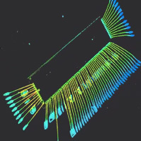
3D Gold Wire Inspection
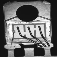
TO Series
Photosensitive Chip
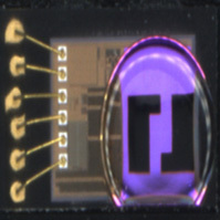
LED Chip
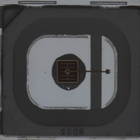
Applications of Leader Scan Products in Different Packaging Types
QFP-Lead Collapse (2D)
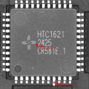
QFP-Lead 3D Measuremen
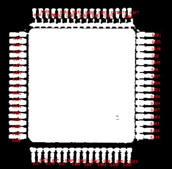
QFN-Foreign Material
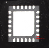
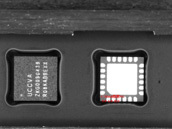
Pre-Seal Inspection - Reel Product
Reversed
BGA- Solder Ball (Pad) Foreign Material
Contamination
