
Classification:
Tiercel-BGL-1520
Welding Line Inspection Equipment
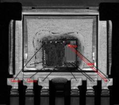
Application: Applied in chip and wire bonding stages, it effectively detects defects in chip appearance and bonding quality.
• Material Clip Binding Function
• 2D/3D Fusion Inspection
• Compatible with Products of Different Materials
Capability
|
Project |
Content |
|
Product Type |
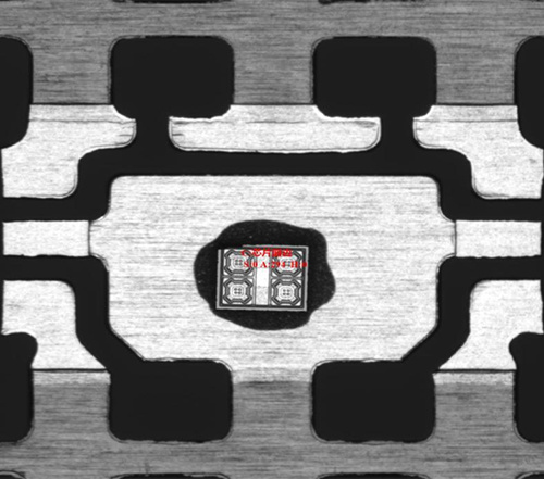
Strip-shaped solder pad, frame and substrate-type solder wire products |
|
Inspection Items |
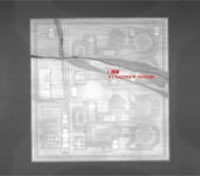
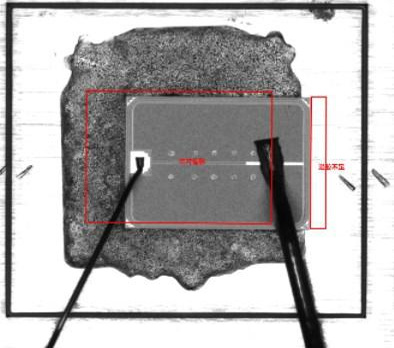
Chip reverse, chip error, chip silver glue/foreign matter, contamination, chip scratch, chip breakage, chip crack, less wire, ball off welding ball offset, broken wire, wire bending, wire tail length, etc |
|
Cutting Path Inspection Items |
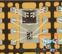
Magazine-style cassettes with track conveyance |
|
Lens and Resolution |
1X lens, resolution: 9344×7000 |
|
UPH |
40-80strips/H (determined by the size of the material strip and the size of the die) |
|
Precision |
5μm/pixel |
|
Optional and Customized |
Mark pen; ink dotting, laser |
Imaging
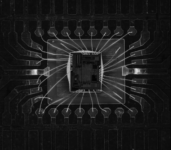 Short Circuit&Wire Breakage |
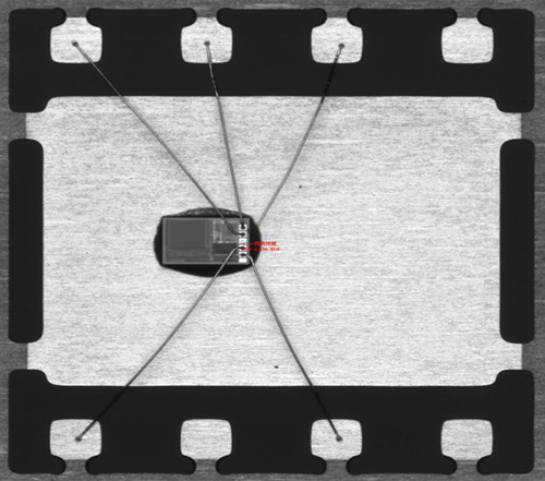 Abnormal Bonding Points |
 Missing wire |
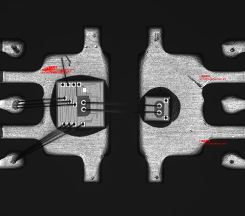 Wire Collapse |
 Hidden Cracks (IR) |
 Die Chipping |
 Die Contamination |
 Chip Misalignment & Lack Solder |
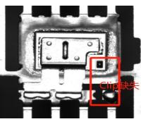 Clip Missing |
 3D Inspection |
- Product Description
-
- Commodity name: Welding Line Inspection Equipment
- Commodity ID: A-003
- 型号: Tiercel-BGL-1520
- 应用: <strong>Application:</strong> Applied in chip and wire bonding stages, it effectively detects defects in chip appearance and bonding quality.
• Material Clip Binding Function<br> • 2D/3D Fusion Inspection<br> • Compatible with Products of Different Materials
Capability
Project
Content
Product Type
Strip-shaped solder pad, frame and substrate-type solder wire products
Inspection Items
Chip reverse, chip error, chip silver glue/foreign matter, contamination,
chip scratch, chip breakage, chip crack, less wire, ball off welding ball
offset, broken wire, wire bending, wire tail length, etc
Cutting Path
Inspection Items
Magazine-style cassettes with track conveyance
Lens and
Resolution
1X lens, resolution: 9344×7000
UPH
40-80strips/H
(determined by the size of the material strip and the size of the die)
Precision
5μm/pixel
Optional and Customized
Mark pen; ink dotting, laser
Imaging
Short Circuit&Wire Breakage
Abnormal Bonding Points
Missing wire
Wire Collapse
Hidden Cracks (IR)
Die Chipping
Die Contamination
Chip Misalignment &
Lack Solder
Clip Missing
3D Inspection
Keywords :
AOI Equipment
Automation
Software Systems
AOI Vision Upgrade
Leave us a message

Jiaxing Jiuzong Intelligent Technology Co., Ltd.
Jiaxing Headquarters
Address: Building 6, Visual Internet of Things Innovation Centre, Tongxiang Economic Development Zone
Ningbo Branch
Address: No.2588, Sanbei Street, Baisha Road Street, Cixi City, Zhejiang Province
Shenzhen Branch
Address: No.27-3, Xintang Road, Fuhai Street, Baoan District, Shenzhen City
Changsha Branch
Address: Wuju Lane, Langli Street, Changsha County, Changsha City
Wuhan Branch
Address: Building 5, Future Light, Optics Valley Avenue, East Lake New Technology Development Zone, Wuhan City

Scan code consultation more
© Jiaxing Jiuzong Intelligent Technology Co., Ltd.